What is a CPU Architecture?
You may have heard the term CPU Architecture, or Computer architecture, but what does it actually mean? Let's find out!
There are three main things that these terms usually refer to, two of which are much more common than the last.
Commercial Performance-Improvement Architecture
The first, and probably most common meaning is the design of a particular release of CPUs from a major company, (for example Zen, Zen+, Skylake, or Alder Lake to name a few). Newer kinds of these architectures generally offer superior performance, or lower power consumption, but fundamentally they use the same design ideas. They might have slightly more ALUs, or a slightly larger cache, better branch prediction, more I/O support, etc, but they are fundamentally the same. There are large differences between different architectures from different companies like AMD and Intel, but they actually have a lot in common as we're about to see:
CPU Use-Case-Adaptation Design
An alternative meaning is the more basic way a CPU is organised, like in the x64 or ARM architectures. These are fundamentally different, and have completely different instruction sets, and they're used for different things. All modern AMD and Intel desktop processors use pretty much the same instructions on an assembly language level, they all use an x64 architecture, and that makes them similar on the most basic level. All x64 architectures have a fairly small number of registers, and many different, complicated instructions that they can run. All ARM processors have a large number of general purpose registers, and a simpler set of instructions. There is one last interpretation, though it's less widely used, and it refers to an even more basic aspect of the way a CPU works.
Memory-Address-Technique Architecture
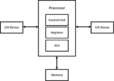
There are 3 types of this kind of architecture, von Neumann, Harvard, and modified Harvard. The differences between them are all in the way that the CPU accesses memory. The first to be implemented was the von Neumann architecture, here both data and instruction memory are combined, and accessed over a single bus:
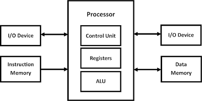
To fix this, a new architecture was devised, the Harvard architecture. The Harvard architecture split memory into two parts which could be accessed simultaneously, one for data, and one for instructions.
This allows for higher performance in specific workloads, and fixed some of the security issues. As the instruction memory cannot be written to, and data can no longer be executed as an instruction. Unfortunately, this exact architecture is rarely used in modern computing, however multiple variations are often used under the term 'modified Harvard architecture'.
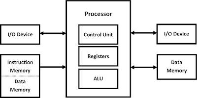
The modified Harvard architectures generally have some separation between data and instruction memory, although there is often some overlap.
Instructions and known data values can be stored in one part of memory, and normal data can be stored in a different memory section. This allows for some simultaneous access of data and instructions, whilst offering slightly more flexibility. Many modern architectures like x86, x64 and ARM use a version of the modified Harvard architecture in their first few levels of Cache, however if the on-chip cache look up in unsuccessful then the von Neumann style link to main system memory will have to be used, slowing down execution speed.
Conclusion
Hopefully that's shed a little more light on the what you're friend/family member/colleague/'random person unnaturally excited computer architectures' was on about! Thank you for reading, and goodbye for now!


Comments
Post a Comment